It's the first time in the history of the world.
The reasoning of the late Renaissance is shattered by a myth.
SemiAnalysis has just released the first third-party logic performance measurement of Google's seventh-generation TPU Ironwood.
Under perfectly equivalent model loads, the TPU's per-dollar performance tops the B200 by as much as 50% and is nearly double the B300's lead by 96%.
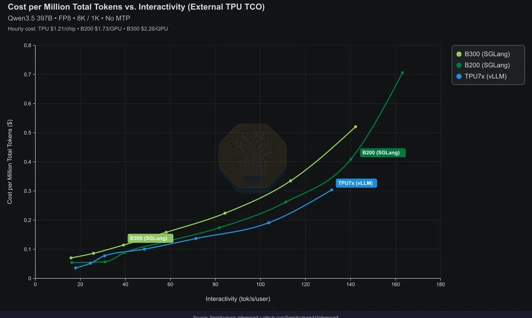 External TCO under the cost per million tokens vs speed of interaction
In return for the industry's most sensitive cost per million tokens, the gap is staggering.
The TPU costs only $0.181, the B200 $0.222 and the B300 $0.276.
More dramatically, it's time.
In April of this year, Huang Rinpoche claimed on the Dwarkesh podcast that neither TPU nor Trainium dared run away. He even publicly encouraged challengers to use InferenceMAX to prove its so-called cost-benefit reasoning.
Today, five months later, the TPU comes up with some of the deadliest data.
Three affirmations by Hu Jintao
In that episode, Huang Rinpoche's disregard for the TPU's strategy can be summed up in three statements.
First, he expressed a great desire to see his opponent prove the cost advantage of the TPU and concluded that this was logically unlikely.
This test method is completely fair and impartial.
The same open-source model, FP8 to FP8, input 8k output 1k, running the B200 and B300 with a load completely consistent with the TPU.
TPU is 19% cheaper than B200 and 34% cheaper than B300 at the single-user throughput benchmark of 100 tokens per second.
If the average response time is 20 seconds, the TPU costs $0.098, the B200 is $0.106, and the B300 rises to $0.132.
The B200 was not defeated on all indicators. It maintained a weak resistance within the narrow 30-second response time zone. However, as the delay demanded relaxation, the TPU regained control of the production high point.
As far as the B300 is concerned, it is entirely at a cost disadvantage.
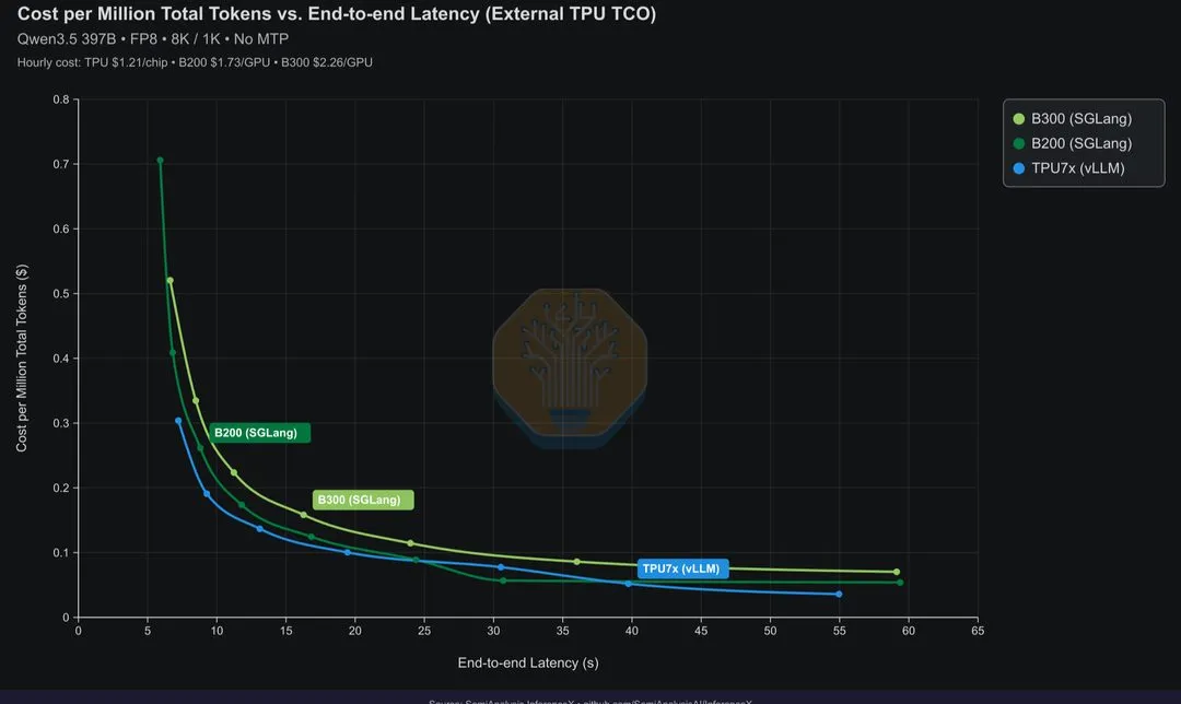 Cost per million tokens vs end to end delay
Second, he claimed that the TPU's advantages were completely unreasonable from the first gender perspective.
Physical testing did not overturn his underlying theory, and Huang Yin was merely miscalculating the calculations of the business world.
For most of its original throughput, the physical performance of the TPU did not match the GPU; however, the TPU's hourly rental costs were abysmally low.
The physical throughput advantage of 5% is superimposed on extremely low unit-time rent, which instantly translates into a 50% per-dollar relative price advantage.
If Google were to calculate the bottom line cost of $1.03 an hour per chip internally, this advantage would be magnified to 77% or even 130%.
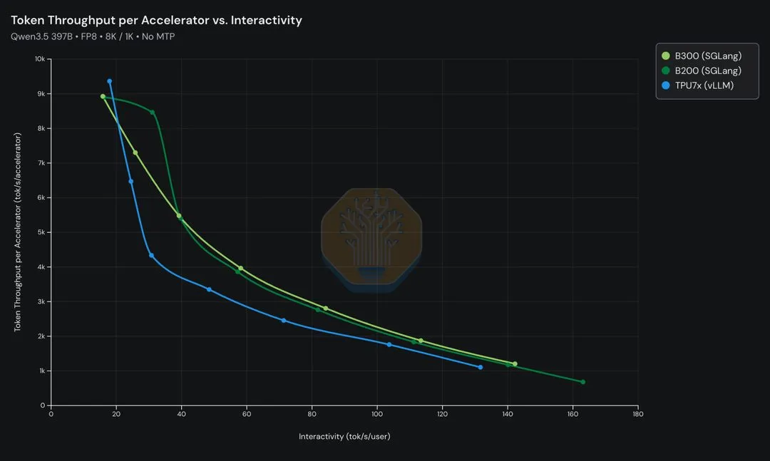 Single-accelerator throughput vs speed of interaction
The absolute calculation of the output of a single chip is calculated, while the actual output that commercial customers can buy is measured by the actual output of each chip.
This open-ended scoring data directly strikes the psychological line of defence on the client side.
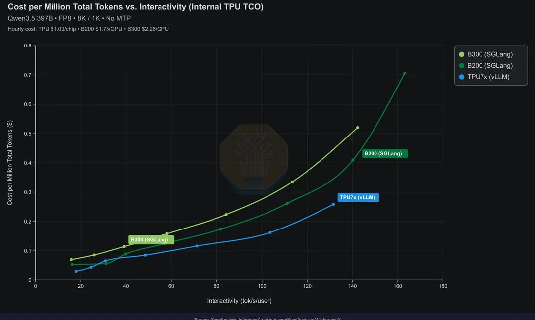 TCO qualities within Google
Third, he concludes that Anthropic is just an exception, and that losing the support of Anthropic will cause the TPU to completely lose its growth engine.
This claim is currently maintained only on the surface.
Anthropic has indeed absorbed more than 1 million TPUs, of which about 400,000 are directly purchased and 600,000 are leased through Google Cloud. By 2029, it will surpass DeepMind to become the world's largest single user of TPUs.
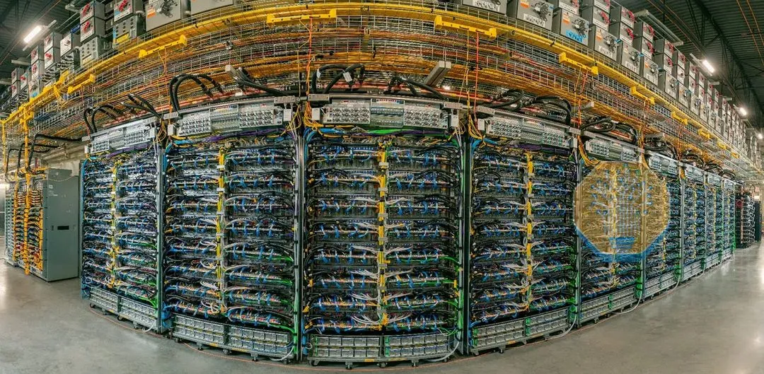
But the other half says it's rapidly failing.
Google has been selling chips directly since last year and is no longer renting out this single pool of clouds. Even researchers inside DeepMind now need to grab computing resources from crowded queues.
In April, Huang Jian said that because TPU has never been overpriced outside.
Now, the price tag has come out, or someone else has traded for Google tags.
TPU's cost of deep water
How does a dedicated chip achieve a cost-saving effect on a general-purpose GPU?
SemiAnalysis, on the other hand, reveals the underlying logic of Google's radically different engineering philosophy.
Google never pursued the physical peak of the chip alone, but instead created a closed-loop system for computing Die, inter-chip connectivity, and the underlying compiler array, compressing the cost of each array in each array.
At the chip level, Ironwood is physically broken down into two separate computing Die, each embedded with two TensorCores and four SparseCores.
Its HBM capacity is six times that of the previous generation Trillium. This number directly determines how big the KV Cache can be, how big the Batch can be.
It was also the first native-generation TPU to support FP8 computing, and it completely said goodbye to previous generations of software simulation compromises.
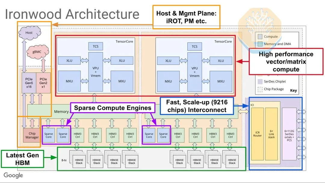
The matrix unit uses a 256×256 pulse array, completing 65536 multiplication operations per cycle, with the computed throughput rising directly to 4 times that of the v5 architecture.
The route to the eighth generation has been further developed: for the first time, Google has broken up training and reasoning into two 8t, 8i chips, and expanded the SRAM on the 8i chips to 384MB, three times as much, leaving the KV Cache specifically for reasoning models on the chips.
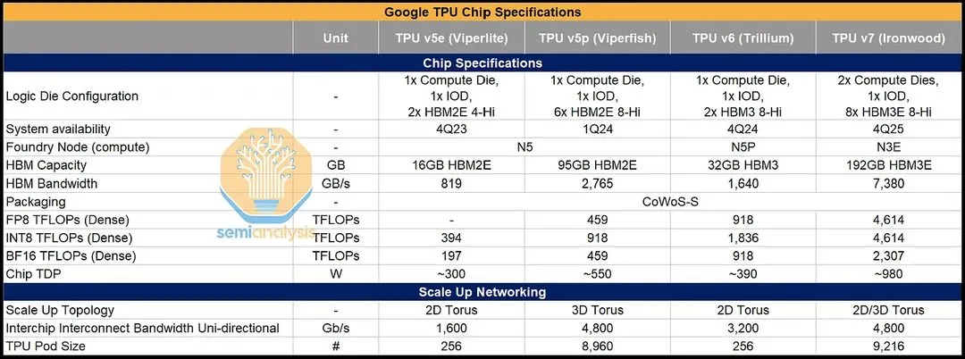 Google TPU comparisons between generations of specifications
In terms of network connectivity, chips interact directly with each other through Google's self-developed ICI mainframe, completely bypassing the host CPU, PCIe, and general network cards.
Its topological structure is in the shape of a 3D Torus, with each chip physically linking 6 adjacent nodes, 64 of which are grouped into a rack-scale cube, and then packed into a super matrix of 9,216 chips via an optical circuit switch.
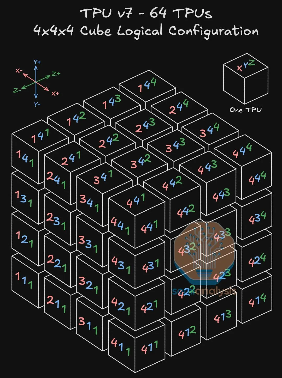 4×4×4 cubic logic configuration of TPU v7
In the event of a failure of any fiber optic link, the system can be re-routed using optical reflectors in seconds without the need for artificial intervention.
By TPU 8i, the 3D Torus would be replaced by the Boardfly topology, and the maximum jump rate under 1,000 chip sizes would be cut from 16 to 7, directly halving the tail delay for each stack of jumps in MoE routes and multicycle agents.
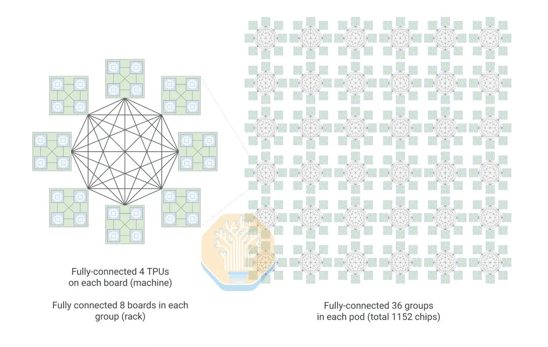
Code-level rebuilding with 50 percent compression efficiencyExtreme performance is often embedded in the violent restructuring of underlying software.
In order to get the first model on the TorchTPU platform up and running, Google, Inferact and RadixArk have spent hundreds of hours working together.
In-depth extraction of a large amount of code can be used to extract three crucial optimizations.
The first is to double the number of pages in KV Cache, significantly reducing the number of token delays.
The TPU vector unit is dealt with in the last dimension of the Tile, which is locked to 128 lanes by the hardware.
The old focus core packs KVs along the head dimension, causing half of the single-KV model to be swallowed up by ineffective complement-zero operations.
Now, Google is moving the Token to the 128 Lane dimension, and the KV page is available from 5141 Storm to 10283.
In parallel 128, throughput increased by 16.5%, the mid-top token delay plunged by 95%, and reasoning requests completely relieved the pain of waiting in line for the KV space.
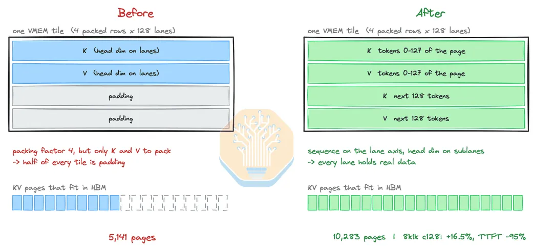 KV cache layout modified before and after contrast
The second is to break down the parameters to improve decoding throughput.
The split-page attention mechanism relies on double buffers to mask HBM latency, which is the simultaneous pre-emption of the next piece of data when computing current data.
The old enabled algorithm locked both computing blocks and reading blocks to 16k tokens, leaving VMEM with no extra space to pre-operate.
Now, the R&D team will keep reading blocks at 16k, computing blocks cut to 4k, and decoding throughput jumps from 64.9k tokens per second to 96.3k.
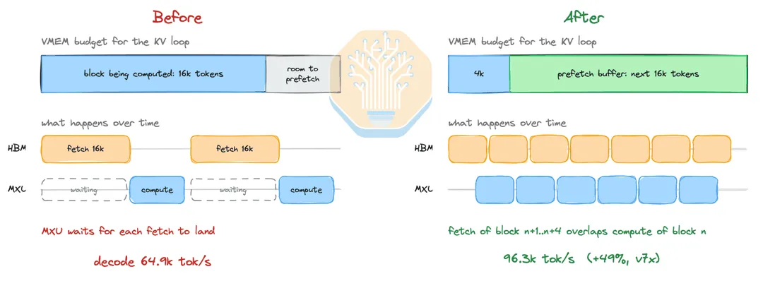 Reading blocks before and after separation of computing blocks
The third is the transfer of communication tasks to SparseCore.
Ironwood's four SparseCores, each equipped with a chip, were originally intended for scarcity calculations such as Embedding checkboards.
Google moved all of the ReducerScatter and MoE's Token rearrangement tasks to SparseCore, freeing up the computing resources of TensorCore to focus on the core matrix multiplication.
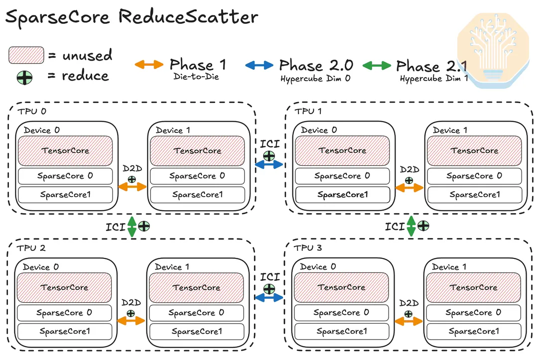 ReduceScatter Phase 3 on SparseCore
At 8k inputs and 1k outputs, throughput increased by 4.1% to 14.2% under load, and at 1k inputs and 8k outputs and concurrent 512 throughput increased by 26.1%.
Hundreds of these tiny but deadly layers of code optimization add up to this overwhelming 50% performance advantage.
Code-level disruption of the Flat-Ecosystem Walled RiverThe most disruptive thing about this update is that Google is just running the software.
The entire open-source reasoning ecosystem was previously deeply rooted in PyTorch and CUDA systems, while TPU's native development environment was JAX.
Previously, vLLM had to run on the TPU using a layer of translation wall called TorchAX, which translated each of the algorithms into JAX one by one at the bottom.
This layer of translation has led to a large number of compatibility issues with sub-page attention and bottom-up optimization, and Google's shared open-source community took more than a year to complete the correction.
Previously used as a JAX/TorchAX service kit
Today TorchTPU directly blows up this translation wall.
It uses PyTorch's proprietary PrivateUse 1 rear-end interface, making the TPU directly a native Torch computing device.
The developers only need to tap the next line of code for the compilation to be handled by XLA, the performance core algorithm calls the Pallas kernel, while the distributed properties such as DDP and FSDP2 run smoothly.
TorchAX path vs TorchTPU native path
For frameworks such as vLLM and SGLang, core code such as the scheduler and API layer can now be directly reused, completely ending the history of rebuilding wheels along high walls.
The vast majority of the Pallas core, which had previously been drilled over a long period of time, could be dropped directly into a completely new environment.
The Imperial Wall of CUDA is made up of two sections. One is the underlying chip performance, and the other is the closed ecological iron curtain.
Today's running score confirms that the irreplaceable nature of its physical performance has been substantially broken.
The ecological curtain that has left countless challengers stranded is being gradually flattened in an irreversible way by the upgrades to PyTorch's underlying architecture.
RoboInd editorial channelResearch, robotics companies and market intelligence for cross-border sourcing.Explore the channel ↗
Share this
End of editorialExplore more from Global Robotics News ↗